ATTENTION! According to the latest data from a reliable source, it became known that not only TTL is the reason for blocking the mobile Internet. If you need information on TTL for routers, and what this protocol affects, then see the last chapter.
Good day to all! Most likely you came here to bypass the blocking of your mobile operator. After all, with the help of TTL, these companies catch the hand of subscribers who have enabled access point mode on their phone. What is TTL? Time To Live is the lifetime of a packet in the IP addressing universe.
When the user turns on the modem or access point mode, the phone starts distributing Wi-Fi along with the Internet. When connecting a computer, laptop, TV, set-top box or other phone (tablet), it is through TTL that the provider understands that the Internet is being distributed to another device.
At the moment, such operators as MTS, Beeline, YOTA, Tele2 and others are guilty of this. As far as I remember, only Megafon has no restrictions yet, but I could be wrong - correct me in the comments if I’m wrong. Next, I will tell you how to find out the TTL value, how to change it, and how to bypass the blocking. Let's start with the theory - I advise you to read it so that everything will be clear to you in the future.
TTL concept
On the Internet, everything is transmitted in packets - small pieces of data. They go from router to router (the same as from router to router) across network nodes. For example, your mobile phone can also become a router if it is used to distribute data to a computer and other devices.
TTL stands for Time To Live, that is, the lifetime of a data packet in seconds. As the packet passes through the next router, the TTL decreases by one. This is necessary so that the packet does not endlessly walk around the network if it cannot reach the addressee. A router that encounters a packet that has reached its TTL value sends an ICMP message to the sender stating that the packet has exceeded the maximum allowed time for being on the network. Maximum TTL=255. Moreover, different operating systems generate packets with different TTLs.
To put it in very simple words... Imagine that you are 5 years old and you want to eat (you are a package). You go to dad and say: “Dad, I want to eat.” Your dad watches TV, according to the routing table, and sends you to your mom. You go to her and ask “Mamaaa, I want to eat.” Mom is chatting with a friend on the phone and, according to her routing table, sends you to dad. And so you walk like a fool from dad to mom and back, back and forth, back and forth, and all because crooked admins (parents of mom and dad) configured the routing table incorrectly. To protect against such situations, they came up with the concept of TTL (Time To Live), which in relation to our situation means the amount of patience a boy has until he says “enough” and falls at the feet of his mother or father in a helpless state. The latter, according to the rules (standards are “this is how it is in the family”), is obliged to send a short unflattering review to the address of the one who sent the boy to eat. This is the so-called “boy is dead” ICMP packet.
Ok, so what do operators have to do with it? The fact is that based on the TTL received from the subscriber, the operator knows whether the Internet is available or not.
Terms: Input/output TTL compatible
TTL (transistor–transistor logic) –
transistor-transistor logic (TTL)
is
a standard of logic elements established since the 60s of the 20th century, built on transistor bipolar technology with a supply voltage of +5 V. A typical basic element of this technology
is
a 2I-NOT logic element of type 7400 ( for example, SN7400 from Texas Instruments or the domestic analogue K155LA3). The schematic diagram of this element is shown in the figure. In subsequent years, logic gate technology was improved while remaining compatible with the previous one. Bipolar technology has been replaced by MOS (CMOS) and other combined silicon technologies. In order to increase performance, families of CMOS, LVTTL logic elements with reduced supply voltages were produced (and are still being produced): 3.3 V, 2.5 V, etc., while the developers of the elements tried by all possible technical means to maintain compatibility according to logical voltage levels with the classic basic TTL element 7400 with a supply voltage of +5 V, since over the past 50 years (!) an unimaginable number of instruments and devices with TTL inputs and outputs have been generated.
We list the main characteristics of TTL inputs and outputs:
Inputs:
- Logical unit voltage level: +2.0…+5.25 V (recommended +2.4…+5.0 V).
- Logical zero voltage level: -0.25…+0.8 V (recommended 0…+0.5 V).
Exits:
- The logical zero voltage is not higher than 0.8 V at an operating output current of 8 mA.
- The logical unit voltage is not lower than 2 V at an operating output current of -0.4 mA.
The characteristics presented above refer to the first TTL elements, which contain a number of imperfections that were subsequently overcome. In particular, most modern CMOS, LVTTL elements already have symmetrical output currents of logic zero and logic one, significantly lower input currents (higher input resistance), some have the property of maintaining a high input resistance when the power is turned off, as well as compatibility with 5-V input levels with its own supply voltage of 3.3 V and below.
In any case, if the documentation indicates “TTL-compatible input or output,” this means to the user that this input (output) belongs to a large family of compatible TTL devices, but in any case, the features of this input and output should be read in the manual to this device.
In addition, the output of any device that connects to a TTL-compatible input must also provide a reasonable voltage drop time (to estimate: no more than the latency of a standard TTL element, which is on the order of 10 ns). It is not recommended to supply a signal with drop durations of more than 10 ns to a regular TTL input (except for a special one with hysteresis), since this can cause a failure (bouncing, ambiguous state) of the input TTL logic element.
It is also important to note that the TTL standard is intended for organizing local short connections (it is recommended –
length less than 0.5 m) in devices having a common wire circuit or a common signal ground.
To increase the noise immunity of TTL lines, electrical matching of lines is used to reduce the wave effects of reflection from unmatched ends of the lines.
If the TTL interface is used to transmit synchronization signals of the measuring system, then, in addition to the requirements for line consistency, the common wire circuits of the transmitter and receiver must be equipotential over a wide frequency band (hundreds of MHz). This is achievable with very good high-frequency connectivity of the common wire circuits of the transmitter and receiver (either these connections must be much shorter than 0.5 m, or the role of the common wire circuit must be performed by an electrically conductive plate or a single electrically conductive chassis of the unit). Such enhanced technical measures are necessary to ensure low introduced phase noise when transmitting synchronization signals.
| Go to other terms | Article created by: | 09.07.2014 |
| About the Terminology section | Latest revision: | 17.08.2019 |
Terms associated with TTL technology of digital devices are used in the documentation of various data acquisition systems, for example, those produced by L Card LLC.
Number of universal inputs/outputs: 32 Number of synchronization signals: 2 Signal type: TTL, 5 V - logic Supply voltage output: ±12 V, 120 mA Additional functions: RS-485 port, a pair of galvanically isolated signals
Digital input/output module 32 inputs/outputs
LTR43
ADC: 16 bit; 16/32 channels; ±0.2 V…10 V; 2 MHz DAC: 16 bit; 2 channels; ±5 V; 1 MHz Digital inputs/outputs: 17/16, TTL 5 V Interface: USB 2.0 (high-speed), Ethernet (100 Mbit) Galvanic isolation.
ADC/DAC module 16/32 channels, 16 bit, 2 MHz, USB, Ethernet
E-502
ADC: 16 bit; 16/32 channels; ±0.2 V…10 V; 2 MHz DAC: 16 bit; 2 channels; ±5 V; 1 MHz Digital I/O: 18/16 TTL 5 V Interface: PCI Express
ADC/DAC board 16/32 channels, 16 bit, 2 MHz, PCI Express
L-502
ADC: 14 bit; 16/32 channels; ±0.15 V…10 V; 200 kHz DAC: 16 bit; 2 channels; ±5 V; 200 kHz Digital inputs/outputs: 16/16 TTL 5 V Interface: USB 2.0
ADC/DAC module 16/32 channels, 14 bit, 200 kHz, USB
E14-140M
ADC: 14 bit; 16/32 channels; ±0.156 V…10 V; 400 kHz DAC: 12 bit; 2 channels; ±5 V; 8 µs Digital inputs/outputs: 16/16 TTL 5 V Interface: USB 2.0
ADC/DAC module 16/32 channels, 14 bit, 400 kHz, USB
E14-440
How do operators know that traffic is being distributed?
Because the subscriber starts receiving packets with different TTL values. There are two reasons for this:
- Firstly, TTL may be different for different devices. And when distributing the Internet, a second device appears - the one to which we distribute the Internet. So, for a phone on iOS or Android, the TTL value is 64, and for a computer on Windows – 128. And when distributing the Internet from the phone to the computer, two different TTL values will appear: 64 and 128. The operator receives packets with both TTL=64 and TTL= 127 (when sending a packet from a computer through a distributing telephone router, the value 128 is reduced by one).
- Secondly, even if the TTL of devices is the same (from phone to phone), the distributing phone again reduces the TTL by 1, like any normal router. And the operator receives packets with different values TTL=64 (if it is a packet from a distributing phone) and TTL=63 (a packet from a consuming phone).
So the operator receives packets with different values:
- TTL of the package from the phone itself.
- TTL of the packet from the device consuming traffic, reduced by one when passing through the router phone.
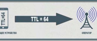
I'm attaching pictures just in case.
This is work without the Internet. The phone transmits only packets with TTL=64 to the operator.
And when distributing the Internet, the phone transmits to the operator packets with three different TTL values: 64 from itself, 127 from the computer and 63 from the consuming phone.
The operator notices such a situation of scattering of TTL values, concludes that traffic is being distributed and takes punitive measures against the violating subscriber who wants to profit from unlimited Internet to the fullest, distributing it wherever he wants. How to hide the distribution from the operator? Obviously, we need to equalize the TTL - bring them all to the same value. To do this you can
- Or change the TTL on the consuming device,
- Or, on the distributing phone, make sure that packets always go to the operator with the same TTL value.
Features of other logics
The basis of the basic logical element of the ESL is the current switch. The current switch circuit (Fig. 3.30) is similar to the differential amplifier circuit.
It is necessary to pay attention to the fact that ESL microcircuits are powered by negative voltage (for example, −4.5 V for the K1500 series). A negative constant reference voltage Uop is applied to the base of transistor VT2. A change in the input voltage uin1 leads to a redistribution of the direct current iе0, specified by the resistance Re between the transistors, which results in a change in the voltages at their collectors.
Transistors do not enter saturation mode, and this is one of the reasons for the high performance of ESL elements.
100, 500 series microcircuits have the following parameters:
- supply voltage −5.2 V;
- power consumption - 100 mW;
- output branching factor - 15;
- signal propagation delay - 2.9 ns.
In n-MOS and p-MOS microcircuits, switches are used, respectively, on MOS transistors with an n-channel and a dynamic load (discussed above) and on MOS transistors with a p-channel.
As an example, consider an n-MOS logic element that implements the OR-NOT function (Fig. 3.31).
It consists of a load transistor T3 and two control transistors T1 and T2. If both transistors T1 and T2 are closed, then the output voltage level is set to a high level. If one or both voltages u1 and u2 are at a high level, then one or both transistors T1 and T2 opens and a low voltage level is set at the output, i.e. the function uout = u1 + u2 is implemented.
To eliminate power consumption by a logic element in a static state, complementary MDP logic elements (CMDP or CMOS logic) are used. CMOS chips use complementary switches on MOS transistors. They are characterized by high noise immunity. CMOS logic is very promising. The complementary switch discussed earlier is actually a NOT element (inverter).
Casting TTL to a single value to bypass operator restrictions
- You can bring the TTL to a single value of 63 by changing it on the distributing phone and on the receiving computer. This is a non-committing TTL change.
Changing the TTL of the sending phone and receiving device
- You can not change anything on the receiving devices, but “force” the distributing phone to always send packets with TTL=63 to the operator, regardless of where they come from: from the distributing phone itself or from the receiving device (computer or phone). This is TTL commit.
TTL fixation
The second scheme is more convenient, but it is not suitable for all phones.
So, we looked at what TTL is and why it needs to be changed. How exactly to change TTL requires consideration in a separate article. How to change TTL on Windows.
Elements of transistor-transistor logic
A characteristic feature of TTL is the use of multi-emitter transistors. These transistors are designed in such a way that the individual emitters do not influence each other. Each emitter has its own pn junction. To a first approximation, a multi-emitter transistor can be modeled by a diode circuit (see the dotted line in Fig. 3.27).
Vasiliev Dmitry Petrovich
Professor of Electrical Engineering, St. Petersburg State Polytechnic University
Ask a Question
A simplified diagram of a TTL element is shown in Fig. 3.27. When we mentally replace a multi-emitter transistor with diodes, we get an element of diode-transistor logic “NAND”. From the analysis of the circuit, we can conclude that if a low voltage level is applied to one of the inputs or both inputs, then the base current of transistor T2 will be zero, and there will be a high voltage level at the collector of transistor T2.
If a high voltage level is applied to both inputs, then a large base current will flow through the base of transistor T2 and a low voltage level will flow at the collector of transistor T2, i.e. this element implements the NAND function:
uout= u1· u2. The basic TTL element contains a multi-emitter transistor that performs logical AND operation and a complex inverter (Fig. 3.28).
If a low voltage level is applied to one or both inputs at the same time, then the multi-emitter transistor is in saturation state and transistor T2 is closed, and therefore transistor T4 is also closed, i.e., the output will have a high voltage level.
Vasiliev Dmitry Petrovich
Professor of Electrical Engineering, St. Petersburg State Polytechnic University
Ask a Question
If a high voltage level is applied at both inputs at the same time, then transistor T2 opens and enters saturation mode, which leads to the opening and saturation of transistor T4 and turning off of transistor T3, i.e. the NAND function is implemented.
To increase the performance of TTL elements, transistors with Schottky diodes (Schottky transistors) are used.
Set the desired TTL value on Android and iOS
To change the lifetime of a data packet on gadgets, we will use special mobile applications that allow you to set the desired value of this indicator in a few seconds. For example, on the Android OS these are “TTL Master”, “Change TTL” (both require root rights to operate).
In the case of iOS, to change the TTL value, simply type in the terminal:
Instead of 65, if necessary, enter any indicator you need.